ZJU scholars develop ultrathin devices for programmable and scalable transfer printing
On June 18, the research team led by Prof. SONG Jizhou from the Zhejiang University School of Aeronautics and Astronautics presented a simple, cost-effective, yet robust transfer printing technique via a shape-conformal stamp with actively actuated surface microstructures for programmable and scalable transfer printing with remarkable reliability and exceptional efficiency. Their research findings are published in a research article entitled “Programmable and scalable transfer printing with high reliability and efficiency for flexible inorganic electronics” in Science Advances.
Flexible inorganic electronic devices have wide applications in wearable health monitoring, deformable displays and human-computer interfaces, thereby capturing immense attention all over the world in the past decade. However, fabricating these unconventional electronic systems relies heavily on the heterogeneous integration of inorganic materials with soft polymeric substrates, which requires the transfer of tiny, ultrathin, and delicate functional components (i.e., inks) from their fabricated rigid wafers to target soft polymeric substrates. This seemingly simple process poses a formidable challenge to the large-scale manufacturing and industrialized application of flexible inorganic electronic devices with the diminishing thickness of functional devices and the soaring number of transfers.
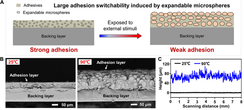
(A) Schematic illustration of the novel concept design to construct a shape-conformal stamp with large adhesion switchability. (B) SEM images and (C) corresponding profile of TRT stamp before and after heating on a hotplate.
The shape-conformal stamp features the polymeric backing and commercially available adhesive layer with embedded expandable microspheres. Upon external thermal stimuli, the embedded microspheres expand to form surface microstructures and yield weak adhesion for reliable release. Systematic experimental and computational studies reveal the fundamental aspects of the extraordinary adhesion switchability of stamps.
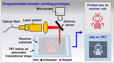
Schematic prototype of the laser-assisted programmable transfer printing system via automated translational stage.
Demonstrations of this protocol involve selective and large-area transfer printing of electronic or optoelectronic components including Si nanomembranes, Si nanomembrane–based photodiodes, and polyimide-based thin film sensors, as well as the manufacturing of ultrathin inorganic LED array–based flexible display. This innovative transfer printing prototype opens up a novel route toward large-area integration of ultrathin and delicate functional micro-objects with high yields in a programmable fashion and could create engineering opportunities in widespread applications such as wearable health-monitoring devices, deformable displays, and heterojunction hybrid electronics.