ZJU scientists delve into second-order susceptibility from ITO-based nanolayer
The electro-optical neural network chip has captured immense attention in both academia and industry, particularly thanks to the substantial competitive edge facilitated by photonics technology. In comparison with electronic AI chips, photonic AI chips exhibit their advantages in two primary aspects. First, they feature lower link loss and higher bandwidth, resulting in higher energy efficiency. Second, optical devices display shorter response times and lower latency compared to traditional electronic devices, rendering them more adaptable for high-speed and real-time calculations in neural networks. However, achieving high performance in on-chip electro-optical neural networks presents a formidable challenge to the nonlinearity of devices, particularly in terms of low loss, integration, and high second-order nonlinear effects.
Recently, a team led by Professors QIAN Haoliang and CHEN Hongsheng from the College of Information Science & Electronic Engineering at Zhejiang University published an article titled “Large second-order susceptibility from a quantized indium-tin-oxide monolayer in the journal Nature Nanotechnology. This groundbreaking work introduces the construction of a metallic quantum well based on a single atomic layer of ITO (indium tin oxide). Through an electronic interband transition resonance in the asymmetric potential energy of the quantum well, a second-order susceptibility χ2 of approximately 1800 pm/V–1 is achieved. This nonlinear coefficient is more than 20 times higher than that of the traditional nonlinear LiNbO3 crystal. This work paves the way for the development and application of key nonlinear optical devices in photonic circuits, especially for ultra-fast modulators for electro-optical neural networks chips.
Thin films of transparent conductive oxides (TCO) are considered ideal low-loss optical materials for photonics circuits due to their high transparency and satisfactory conductivity. Moreover, the tunability of their electrical and optical properties enables the multifunctionality of TCO-based devices, thanks to the moderate charge carrier density. One of the most frequently used TCOs is ITO, known for its high visible transmission of over 80%, an electron concentration of over 1021 cm-3, and compatibility with the complementary metal–oxide–semiconductor fabrication method. It is also regarded as a potential candidate for low-loss photonic circuit applications. However, ITO films with a thickness of several micrometers exhibit limited dipole transition moments, resulting in a weak χ2 due to their centrosymmetric lattice structure.
The magnitude of nonlinear effects in materials is proportional to the second-order susceptibility χ2, which is chiefly determined by two critical parameters: the dipole dephasing rate and the dipole transition moment. Therefore, to enhance the optical nonlinear susceptibility, it is imperative to reduce optical losses and increase dipole transition moments. To further increase second-order nonlinear effects in asymmetric materials, a common approach involves increasing light-matter interactions based on electric-field enhancement. However, this method has a potential upper limit on the electric field enhancement and requires complex optical design and nanofabrication. Another approach is to engineer electronic energy bands to induce dipole transition resonance, which could create an effectual optical nonlinear susceptibility enhancement of several orders of magnitude. Therefore, the research team proposed an ITO metallic quantum well with asymmetric potential through van der Waals forces. By leveraging the low-loss optical properties of the ITO metallic quantum well and achieving large-bandgap interband transitions (IBT) and intraband transitions (ISBT), the second-order susceptibility χ2 of approximately 1800 pm/V–1 was achieved.
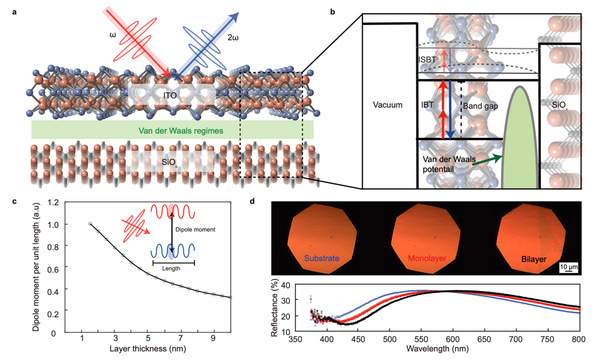
Fig. 1: Second-order nonlinearity in van der Waals 2D ITO films.
Signal processing based on electro-optical neural network chips may well revolutionize the performance of classical electronic computing and communication devices. On-chip high-performance nonlinear devices, such as reconfigurable nonlinear activation functions and ultra-fast MZ modulators, are crucial for high-speed signal processing in electro-optical neural network chips. They not only bring about significant improvements in chip integration, speed, and efficiency but also lead to breakthroughs in chip capabilities and functions. Moreover, advancements in on-chip nonlinear devices also serve as a cornerstone for subsequent neural network chip designs based on quantum on-chip networks.