World’s first electrically-driven perovskite laser


Semiconductor lasers are critical light sources for information technologies, but their fabrication processes are often complicated and costly. There are some solution-processable lasing materials, such as organic, quantum dot and perovskite semiconductors, which can be easily integrated with the mass-produced silicon platforms at low cost. Among these materials, perovskite semiconductors stand out as an exceptional class owing to their ability to achieve surprisingly low threshold lasing under optical pumping.
However, optically-driven lasers are not very useful in practical applications, as bulky external light sources (such as pulsed lasers) are still needed. Historically, the success of conventional semiconductor lasers was built on the ability of electrically driving the lasing action. For perovskite lasers, realizing electrically-driven lasing stands as a grand challenge in the field, despite the intensive worldwide research efforts over the past decade.
Recently, researchers at Zhejiang University invented an electrically-driven perovskite laser. It is a dual-cavity laser created by integrating a low-threshold perovskite single-crystal microcavity sub-unit with a high-power microcavity perovskite LED sub-unit, featuring a vertically stacked multi-layer structure. Operating under electrical excitation, the device shows a lasing threshold of 92 A/cm2, which is an order of magnitude lower than that of the best electrically-driven organic lasers. The perovskite laser shows superior stability compared to the organic lasers, and can be rapidly modulated at a bandwidth of 36.2 MHz. This new class of lasers may find their use in on-chip data transmission, computation and biomedical applications.
The related research paper entitled “Electrically driven lasing from a dual-cavity perovskite device” was recently published in Nature (Zou et al, Nature (2025), https://doi.org/10.1038/s41586-025-09457-2). The corresponding authors of the paper are Prof. DI Dawei, Dr. ZOU Chen and Prof. ZHAO Baodan of Zhejiang University. The first author of the paper is Dr. ZOU Chen.
Figure 1: Structure of the electrically-driven perovskite laser. Source: Nature (2025).
“This is a remarkable breakthrough”, said Prof. DI Dawei, Deputy Director of the International Research Center for Advanced Photonics of Zhejiang University. “Realizing electrically-driven perovskite lasers has been long considered to be the greatest challenge in the field of perovskite optoelectronics, and it is the common goal of numerous research groups around the world. In our latest work, we addressed this challenge by using an integrated dual-cavity device structure. Under electrical excitation, the lasing threshold of our perovskite laser is an order of magnitude lower than the best electrically-driven organic lasers. The lasing properties were rigorously tested, showing good reproducibility and stability”, said Di.

Figure 2: Performance of the electrically-driven perovskite laser. Source: Nature (2025).
“To enable electrically-driven lasing, we came up with a dual-cavity structure”, said Dr. ZOU Chen. “Our idea is to compactly integrate a high-power microcavity perovskite LED sub-unit with a high-quality single-crystal perovskite microcavity sub-unit in the same device. The device architecture may seem to be complex, but the design principle is easy to explain. The integrated laser device includes two microcavities that are optically coupled at a high efficiency of 82.7%. Under electrical pulses, the microcavity perovskite LED sub-unit produces a peak radiant exitance of ~2.5×10⁴ mW/cm2, which is equivalent to an exceptionally high radiance of ~2.0×10⁵ W/sr/m2. The concentrated optical power is efficiently delivered into the single-crystal perovskite microcavity to support the lasing action,” said Zou.

Figure 3: The advantages of the dual-cavity device structure. Source: Nature (2025).
“The perovskite laser can be used in various applications such as optical data transmission”, said Prof. ZHAO Baodan. “We found that the device can be rapidly modulated by electrical pulses at a bandwidth of 36.2 MHz. This modulation rate was achieved by reducing the device active area for minimum RC constants, and by using a silicon substrate for improved heat dissipation”, said Zhao. “In the future, we need to overcome the limitation of the nanosecond spontaneous emission lifetimes of the microcavity perovskite LED sub-unit to achieve faster, GHz operation using the perovskite lasers.”, she said.
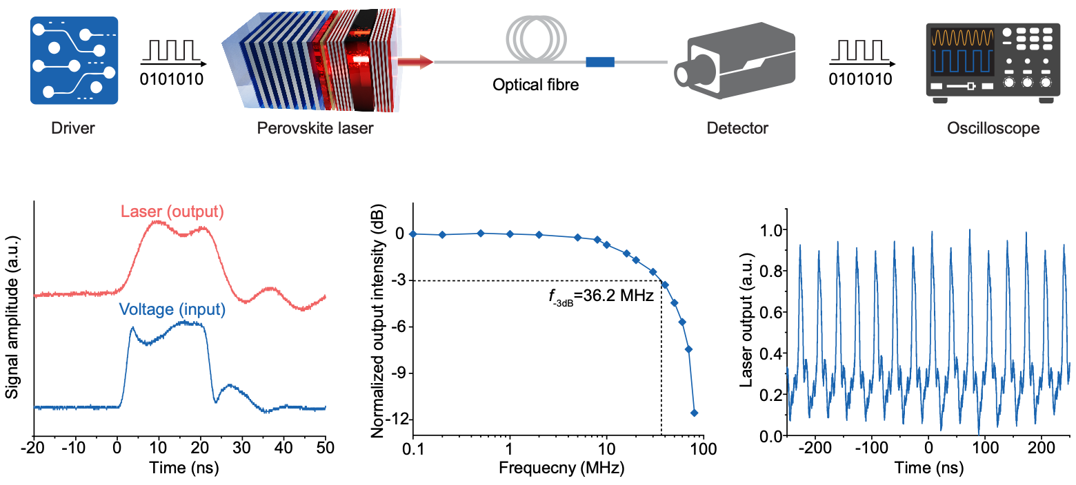
Figure 4: Optical data transmission using the perovskite laser. Source: Nature (2025).
“We anticipate that there will be many other applications of the perovskite lasers”, said Zou, “for example, they may be used as a coherent light source in integrated photonic chips and wearable devices”. The demonstration of the electrically-driven perovskite lasers is just the beginning. There are many difficulties to overcome to improve this new laser technology toward real-world applications. “The transition from an ‘integrated pumping’ architecture we currently use to a simple laser diode structure would be an important next step, as this would enable more compact and scalable optoelectronic applications. We are glad to achieve the initial milestone, and are prepared for the great challenges ahead”, said Di.
Related paper:
Zou, C. et al, Electrically driven lasing from a dual-cavity perovskite device. Nature (2025). https://www.nature.com/articles/s41586-025-09457-2
Source: Prof. DI Dawei, Dr. ZOU Chen, Prof. ZHAO Baodan and co-authors; Nature (2025).